CHIPS of Europe: Building Semiconductor Expertise for the Next Generation
Europe’s sovereignty in semiconductor technology depends not only on fabrication facilities and investment, but above all on highly skilled engineers who truly understand the physics of modern devices.
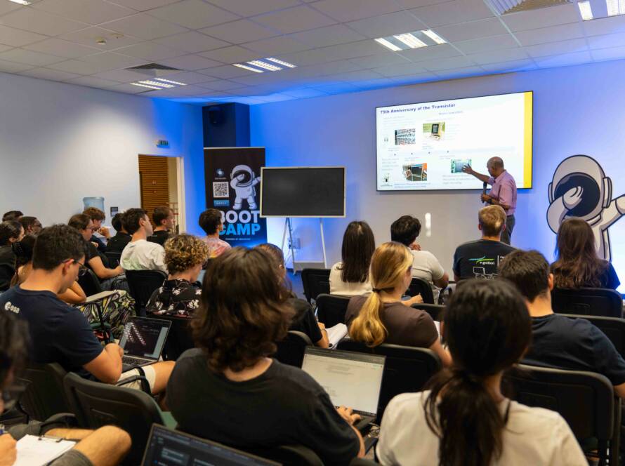
This is precisely where the CHIPS of Europe project comes in. It brings together academic institutions, industry partners, and educational organisations from across Europe to provide the next generation of microelectronics specialists with hands-on, high-level training.
A key component of this initiative is the Virtual Lab – a virtual learning environment in which students can not only study semiconductor devices theoretically, but also simulate and explore their behaviour directly.
nextnano contributes its simulation software and expertise in device physics to this Virtual Lab. The aim is to make complex semiconductor physics accessible without oversimplifying it, thereby fostering an understanding that goes beyond circuit-level intuition.
A Common Misconception: Current and the Elctric Field
A simplified concept frequently arises in the education of electrical engineering and physics students: current in a transistor is primarily driven by the electric field.
This statement is not incorrect – but it is incomplete.
In reality, the electric field describes only the drift component of the charge carrier current. Particularly in microscopic devices such as modern transistors, this perspective alone is insufficient to accurately explain their actual behaviour.
The Physically Correct Perspective: The Quasi-Fermi Level Gradient
The total charge carrier current is not determined solely by the electric field, but by the gradient of the quasi-Fermi level.
For both electrons and holes, current flows precisely when their respective quasi-Fermi levels vary spatially.
This gradient naturally combines two physical mechanisms:
- Drift – caused by the electric field
- Diffusion – caused by charge carrier concentration gradients
The more precise and generally applicable statement is therefore:
Current flows because the quasi-Fermi level changes with position.
Without a quasi-Fermi level gradient, no current flows; if the gradient is finite, current flows – regardless of whether drift or diffusion dominates.
Why This Distinction Matters for Device Simulation
Although this refinement may appear academic at first glance, it has significant practical implications – particularly for the simulation of modern semiconductor devices, as taught within the CHIPS of Europe Virtual Lab.
In highly scaled modern transistors, charge carrier densities can vary substantially over extremely short distances. Under these conditions, diffusion is not a negligible correction term but often a key mechanism governing device behaviour.
Those who think exclusively in terms of electric fields risk misinterpreting simulation results or overlooking important effects – especially in situations where concentration gradients dominate charge transport.
By contrast, thinking in terms of quasi-Fermi levels provides a clear and consistently applicable physical framework that can be directly transferred to the interpretation of simulation data:
- No quasi-Fermi level gradient → no current flow
- Finite quasi-Fermi level gradient → current flow
This understanding is precisely what distinguishes circuit-level intuition from a robust understanding of device physics – a distinction that is becoming increasingly important for the development of future semiconductor technologies.
From Physical Concept to Practical Simulation
Within the CHIPS of Europe Virtual Lab, nextnano aims to do more than simply provide students with a tool for semiconductor device simulation.
The objective is to develop the right physical intuition together with learners:
- What actually drives current?
- How do drift and diffusion interact?
- Why can device behaviour not always be reduced to a simple field-based picture?
By enabling students to explore these relationships directly through device simulations, the Virtual Lab creates an understanding that extends far beyond applying equations mechanically.
And that is exactly the foundation required for the next generation of semiconductor expertise in Europe.