The semiconductor industry needs highly skilled graduates who understand not only the theory behind micro- and nanotechnology, but also how this knowledge is applied in real industrial environments. This is exactly where CHIPS of Europe comes in.
The project aims to develop and strengthen study programmes that reflect the real needs of the semiconductor industry. By combining theoretical learning with practical training at Bachelor and Master level, CHIPS of Europe helps prepare students for careers in one of Europe’s most strategically important technology sectors. This aligns with the project’s broader goal of building a sustainable talent pipeline for Europe’s semiconductor industry and increasing the attractiveness of semiconductor-related studies and careers.
From Theory to Cleanroom: A Real-World Lab Class at Hochschule München
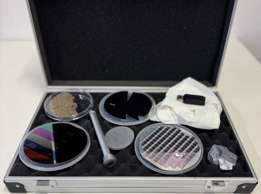
A strong example of application-driven teaching is the Lab Course Microtechnology offered within the Master programme Micro- and Nanotechnology at Hochschule München University of Applied Sciences.
In this lab class, students design, fabricate, assemble, and characterize a surface acoustic wave filter. These tiny components play a major role in everyday technology: smartphones contain many such filters to separate frequencies, enabling mobile devices to handle multiple wireless signals and applications at the same time.
Study programme link:
https://sci.hm.edu/studierende/studiengaenge/master/micro_and_nanotechnology/index.en.html
Industry and Academia Working Side by Side
The lab course is developed in close collaboration with the local industry partner Qualcomm, where these types of filters are designed and fabricated. Students begin with a theoretical introduction delivered by a company representative, covering filter functionality, design, fabrication, and real-world applications.
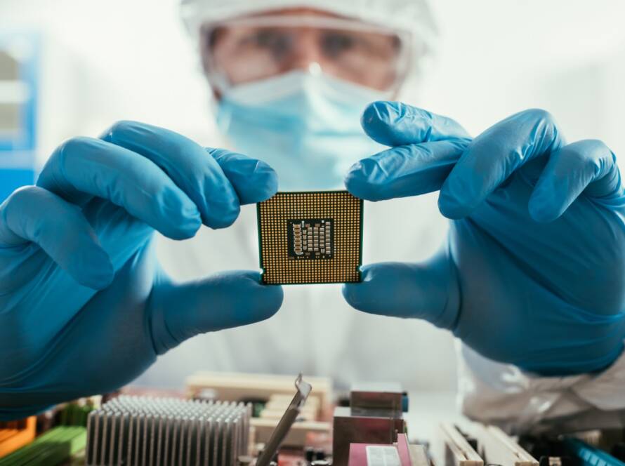
They then move from theory to practice by designing their own filters and fabricating them in the HM cleanroom. After assembly, students characterize the filters using optical methods, scanning electron microscopy, and electrical measurements. This allows them to understand how small deviations in the fabrication process can influence frequency response and bandwidth.
Why This Matters
This lab class demonstrates how effective semiconductor education can be when universities and companies collaborate closely. Students gain hands-on experience across the full process chain: design, microfabrication, assembly, and analysis.
For the semiconductor sector, this type of education is essential. It helps ensure that graduates are not only technically knowledgeable, but also ready to contribute to interdisciplinary, industry-relevant projects from the start of their careers.