
Modern life depends on semiconductors. They power our smartphones, cars, renewable energy systems, medical devices, industrial machines, and AI applications. But before a chip can make any of this possible, it has to be manufactured with extraordinary precision.
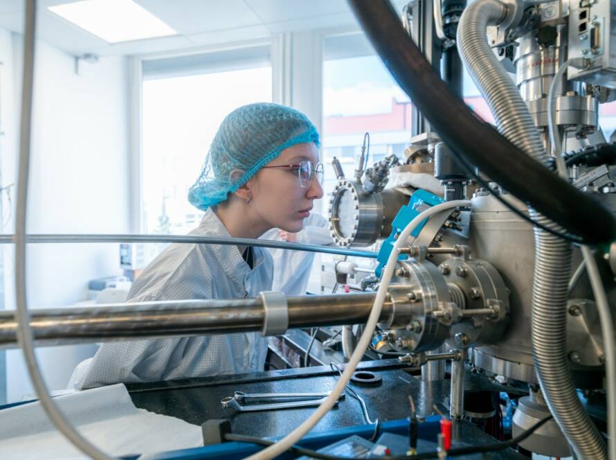
Step inside a modern semiconductor fab and you enter a world where the smallest details matter. Here, engineers work at the nanometre scale, creating structures far smaller than the width of a human hair. One of the key technologies behind today’s most advanced chips is Extreme Ultraviolet lithography, better known as EUV lithography.
What is EUV lithography?
EUV lithography uses light with a wavelength of just 13.5 nanometres to create extremely fine patterns on silicon wafers. A simple way to imagine this is to think of drawing a picture. If you use a thick marker, you can only create broad lines. If you use an ultra-fine pen, you can draw much smaller and more detailed structures.
That is what EUV makes possible in semiconductor manufacturing. It enables smaller chip features, more transistors, higher performance, and improved energy efficiency. This is essential for the next generation of technologies, from artificial intelligence to electric mobility and cleaner industrial systems.
A complete ecosystem of precision engineering
EUV lithography does not work alone. Around it stands a highly advanced ecosystem of semiconductor technologies and expertise.
This includes photoresists and masks, which help transfer patterns onto wafers, as well as deposition and etching systems, which build up and shape ultra-thin layers of material. Advanced metrology tools continuously measure alignment, dimensions, and quality at nanometre scale.
Every step must be carefully controlled. Even the smallest deviation can affect the performance of a chip. That is why modern fabs rely on sophisticated control software, increasingly supported by artificial intelligence.
These systems monitor production in real time. They measure, model, and optimise processes to improve quality, increase yield, and reduce waste.
Sustainability in semiconductor manufacturing
Precision manufacturing also comes with responsibility. Semiconductor production requires resources such as ultra-pure water, energy, and specialist materials. This makes sustainability an important focus across the semiconductor value chain.
Modern fabs are working to reduce their environmental impact by recycling ultra-pure water, recovering heat, reducing process emissions, and improving production yield. Higher yield means fewer defective chips, less wasted material, and more efficient use of resources.
Sustainable semiconductor manufacturing is not only about reducing emissions. It is also about designing smarter processes, using materials responsibly, and building technologies that support the green and digital transition.
Europe’s role in semiconductor innovation
Europe plays a leading role in several key areas of semiconductor technology. This is especially true for EUV technology, optics, metrology, materials science, and semiconductor research.
European companies, universities, and research institutes contribute essential knowledge and technologies to the global semiconductor ecosystem. Their expertise supports the development of smaller, faster, and more energy-efficient chips.
As demand for advanced semiconductors continues to grow, Europe’s strengths in precision engineering and research are becoming increasingly important. From AI and smart mobility to renewable energy and cleaner industry, semiconductor innovation begins with precise, responsible manufacturing.
Why it matters
Semiconductors may be tiny, but their impact is enormous. They are at the heart of digital transformation, industrial innovation, and climate-friendly technologies.
Inside the cleanroom, every nanometre counts. Through EUV lithography, advanced process control, sustainable manufacturing, and strong European expertise, the semiconductor industry is shaping the technologies of tomorrow.
Keywords integrated: EUV lithography, semiconductor manufacturing, semiconductor fab, cleanroom, Europe semiconductor industry, sustainable semiconductor manufacturing, metrology, optics, materials science, AI in semiconductor manufacturing.