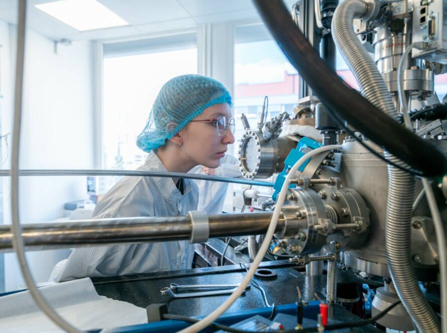
Hands-on laboratory experience is essential in semiconductor education. But lab time is often limited, and complex tools require careful preparation. This is where the Virtual Laboratory for Semiconductors, or VLabS, comes in.
Developed within the CHIPS of Europe project, VLabS makes selected semiconductor laboratory tools accessible online. The aim is to help students prepare for practical lab classes virtually before working with the real equipment on site. By exploring lab processes in advance, students can use their time in the physical laboratory more efficiently, safely, and confidently.
First VLabS modules are already online
The first VLabS modules are already available and give students an early impression of virtual semiconductor training. Two modules focus on key processes in semiconductor assembly technology:
Screen printing and wire bonding.
Both processes play an important role in the Master’s programme Micro- and Nanotechnology at Hochschule München University of Applied Sciences. They are part of the mandatory Lab Class Microtechnology, where students design, fabricate, and characterize a surface acoustic wave filter.
In this lab class, students do not only need to design the right comb structure for the required frequency and bandwidth. The filter also needs to be assembled into a package so that it can be electrically analyzed. For this, screen printing is used to prepare a chip carrier, while wire bonding is used to connect the chip to the carrier.
Learning anytime, anywhere, and at your own pace
The virtual experiments are designed to complement in-person laboratory work. Students can repeat the modules as often as they want, work through them at their own pace, and access them from anywhere.
This flexible approach supports better preparation before entering the lab. It also helps students understand complex semiconductor manufacturing and assembly processes before using real tools.
A first version of the screen printer is now also available as a VR experience, making the virtual training even more realistic. This immersive format helps students become familiar with the tool and its workflow before operating the real machine.
Through VLabS, the CHIPS of Europe project contributes to modern, accessible, and practice-oriented semiconductor education — preparing students for the skills needed in Europe’s semiconductor industry.
Learn more about VLabS:
https://sci.hm.edu/forschung/labore/vlabs/vlabs_1.en.html
Learn more about the Master’s programme Micro- and Nanotechnology:
https://sci.hm.edu/studierende/studiengaenge/master/micro_and_nanotechnology/index.en.html