Europe’s competitiveness in semiconductors depends not only on technological innovation, but also on educating the engineers and researchers who will drive future breakthroughs. Developing the next generation of talent requires access to modern facilities, advanced manufacturing technologies, and practical training that complements theoretical education.
This is one of the key objectives of the CHIPS of Europe project. By bringing together universities, research organisations and industrial partners from across Europe, the project aims to strengthen semiconductor education, foster collaboration, and equip students with the knowledge and practical skills required by Europe’s rapidly evolving microelectronics sector.
A significant milestone towards this goal has recently been achieved at the Centre for Nanoscience and Nanotechnology (C2N) at Paris-Saclay University. Through CHIPS of Europe, C2N has acquired and installed a state-of-the-art µMLA laser lithography system from Heidelberg Instruments, expanding the capabilities of its dedicated training clean room.
Beginning in autumn 2026, students will have the opportunity to design, pattern and fabricate their own microelectronic devices using professional semiconductor manufacturing equipment. This new capability provides a level of autonomy and practical experience that has not previously been available within the laboratory courses.
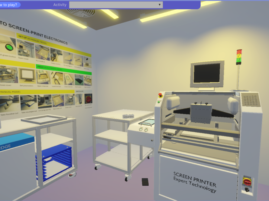
Practical training plays a crucial role in semiconductor education. While theoretical knowledge forms the foundation, understanding fabrication processes and gaining experience with industry-relevant equipment are essential for preparing students for careers in research and industry. By working directly with advanced lithography technology, students will develop valuable skills in microfabrication and device processing that reflect real-world semiconductor manufacturing environments.
The installation of the new laser lithography system represents another important step towards creating modern educational infrastructures across Europe. Investments in advanced laboratory equipment not only enhance the quality of university education but also contribute to strengthening Europe’s semiconductor ecosystem by preparing a highly skilled workforce for future technological challenges.
CHIPS of Europe is proud to support initiatives such as this and would like to thank all partners involved for their collaboration and commitment to advancing semiconductor education throughout Europe.