Europe’s semiconductor sector needs more skilled professionals. To build a stronger talent pipeline, students need opportunities to connect academic learning with real industrial challenges early in their education.
This is one of the key goals of CHIPS of Europe: strengthening collaboration between higher education and industry to make semiconductor careers more visible, attractive, and relevant.
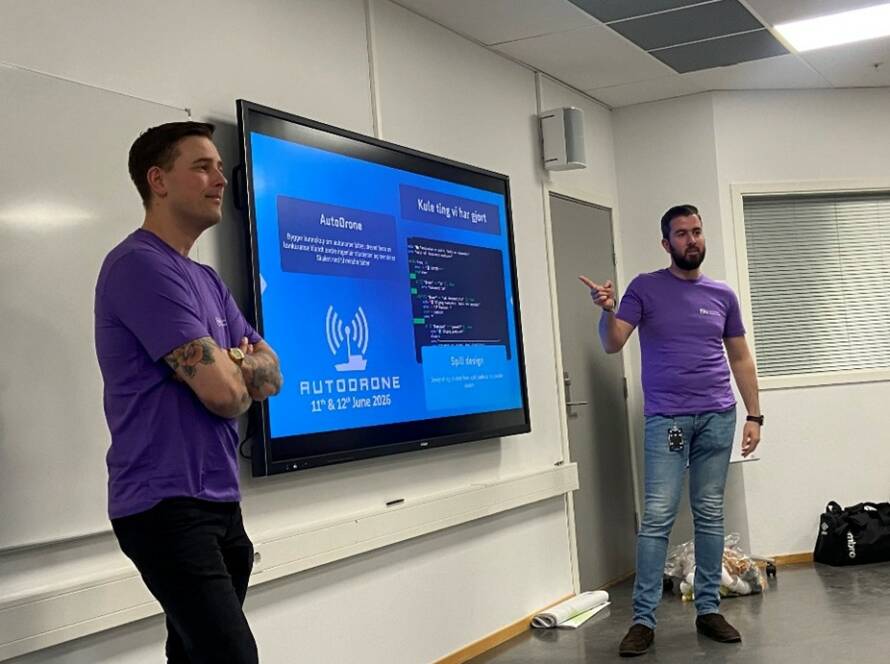
One practical example comes from the Industrial Master programme at the University of South-Eastern Norway (USN). This programme connects university studies directly with industry work. Students are employed 50% in a company while completing their Master’s degree, allowing them to contribute to real development projects while continuing their academic training.
What makes an Industrial Master programme different?
An Industrial Master programme is not a standard MSc pathway. It is a structured collaboration between a university and an industry partner, designed to give students hands-on experience in a professional environment.
Students are not simply observing from the outside. They become part of development teams, work with industry tools, and contribute to technical challenges that matter for real products and applications.
This type of setup is still not common across European universities. That is what makes it a valuable complement to traditional study programmes. It creates a direct link between education, research, and product development, instead of treating them as separate tracks.
A real-world example: ASIC design for medical ultrasound technology
At GE HealthCare, one Industrial Master student from USN is integrated into an ASIC design team working on electronics for ultrasound probes.
The work involves custom digital and analogue ASIC design, with typical engineering constraints around performance, power consumption, and reliability. These are not simplified student exercises. The student works with the same tools, data, and challenges as the rest of the team.
Her contribution has already been concrete. She has supported the analysis of Electrical Wafer Sort data to improve understanding of chip quality and yield. She has also contributed to Multi-Project Wafer layout preparation, aligning her work with both ongoing development activities at GE HealthCare and her MSc thesis.
This model shows how semiconductor students can gain meaningful industry experience while companies benefit from early access to relevant skills and academic insight.
Connecting technical work with outreach
The student has also been involved in outreach and collaboration activities with the university. As part of this, she has contributed to the TogetHER in TECH initiative, where she has shared her perspective on entering the technology field and given a presentation explaining how ultrasound works.
This kind of activity is valuable because it connects education, industry, and public engagement. It also helps make technology more accessible to students who may not yet see themselves in semiconductor-related careers.
For initiatives such as CHIPS of Europe, this is especially relevant. Building the future semiconductor workforce is not only about developing technical skills. It is also about making the field more visible, inclusive, and attractive to the next generation.
Why industry-academia collaboration matters for semiconductor skills
From a company perspective, Industrial Master programmes provide early access to emerging talent. They make it possible to connect academic work directly with real industrial needs in areas such as ASIC design, sensor systems, chip testing, and product development.
From the student’s perspective, the model offers practical experience with real engineering work, including the complexity and constraints that come with industrial development. The gap between learning and application becomes smaller.
For universities, this type of collaboration strengthens the relevance of semiconductor education. It creates feedback loops between curricula, research, and industry practice, helping students prepare for the skills needed in Europe’s semiconductor ecosystem.
Supporting Europe’s semiconductor talent pipeline
For CHIPS of Europe, examples like this show why closer cooperation between universities and companies matters.
Building semiconductor competence in Europe is not only about technology. It is also about people. Industrial Master programmes help students develop practical skills in fields such as ASIC design and sensor systems, while strengthening long-term collaboration between academia and industry.
They offer a practical model for connecting education with real semiconductor work. By combining academic learning with hands-on development experience, they help prepare students for future careers and support Europe’s ambition to build a stronger, more sustainable semiconductor talent pipeline.
An Industrial Master programme is a study model where students combine academic Master’s-level education with part-time employment in a company. This allows them to gain practical industry experience while completing their degree.
Semiconductor development requires highly specialised skills. Industrial Master programmes help students apply academic knowledge to real challenges in areas such as chip design, ASIC development, testing, reliability, and sensor systems.
Students gain hands-on experience, work with professional tools, and understand the technical and organisational complexity of real development projects. This helps them transition more easily from university to industry.
Companies gain early access to skilled students, strengthen collaboration with universities, and can connect academic research more directly with industry needs.
CHIPS of Europe aims to strengthen Europe’s semiconductor talent pipeline by connecting schools, universities, and industry. Industrial Master programmes are one example of how this collaboration can work in practice.