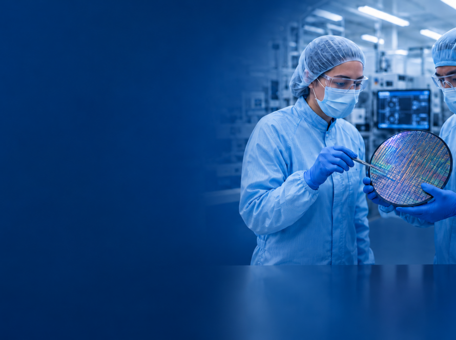
How are computer chips actually made? What happens inside a semiconductor cleanroom? And how can we bring this highly specialized world into classrooms and living rooms across Europe?
The CHIPS of Europe project is taking a major step toward answering these questions with VLabS – the Virtual Laboratory for Semiconductor Technology. Version 1.2 of the virtual lab was officially released on 21 October 2025, offering an immersive, game-based learning experience designed to spark curiosity, teach core fabrication processes, and make Europe’s semiconductor landscape more accessible than ever before.
What Is VLabS?
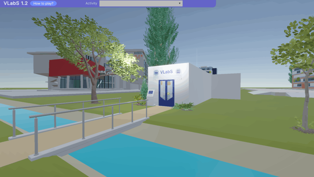
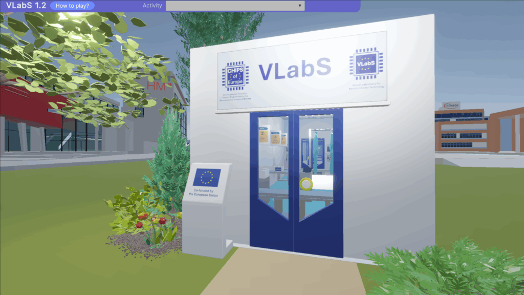
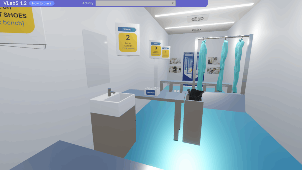
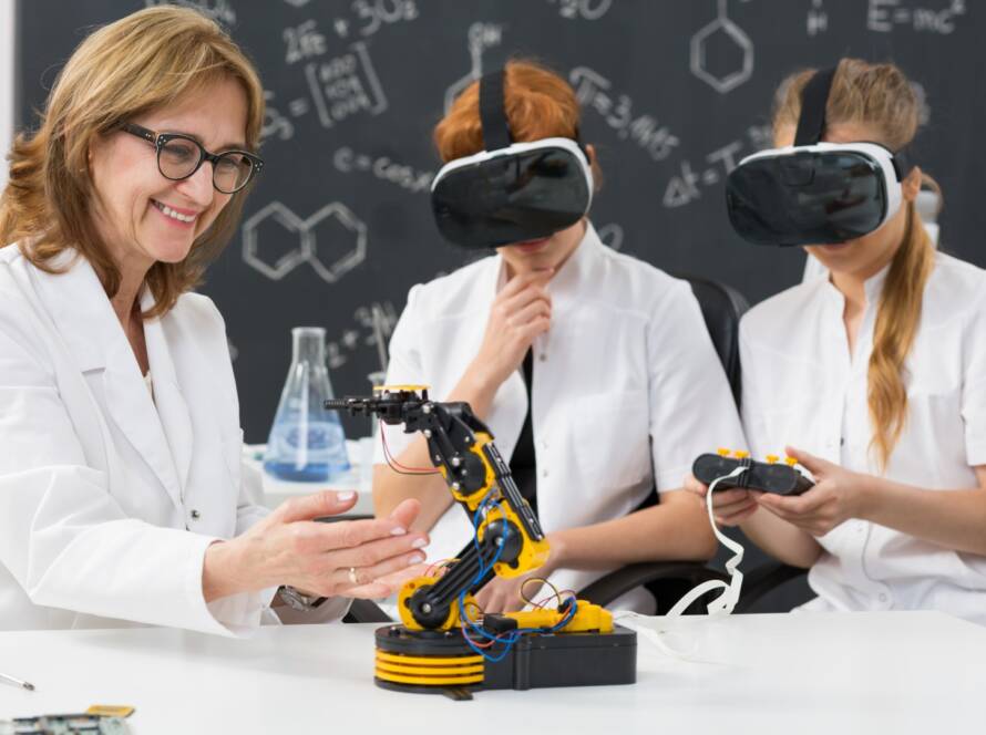
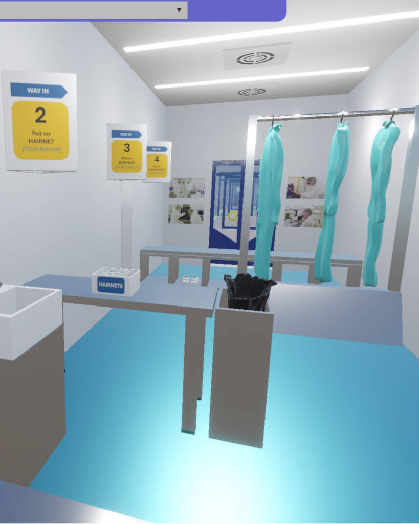
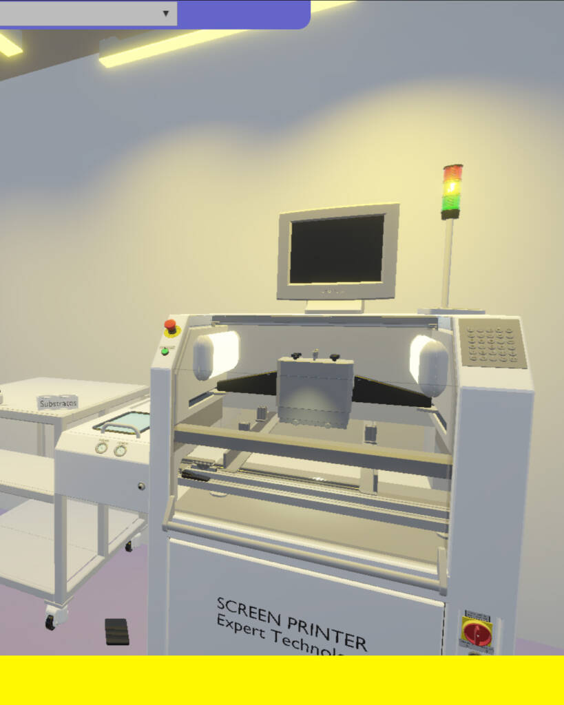
VLabS is a work-in-progress virtual laboratory that functions like a computer game. Players move through a digital cleanroom environment and experiment with tools and processes used in chip fabrication. Each station is modeled after real semiconductor equipment, allowing learners to understand complex processes through interactive, hands-on exploration.
VLabS is targeted at the general public, high-school students, and university students, giving each group an intuitive entry point into the world of micro- and nanotechnology.
Current Status: VLabS 1.2
Version 1.2 includes a growing collection of completed lab modules as well as faithfully reconstructed 3D models of real European semiconductor sites. The aim is to teach semiconductor technology step by step, while connecting the digital experience to recognizable campuses and companies.
Completed Lab Modules
Players can already explore and interact with five fully developed semiconductor process steps:
Airlock – Introduction to cleanroom etiquette and procedures
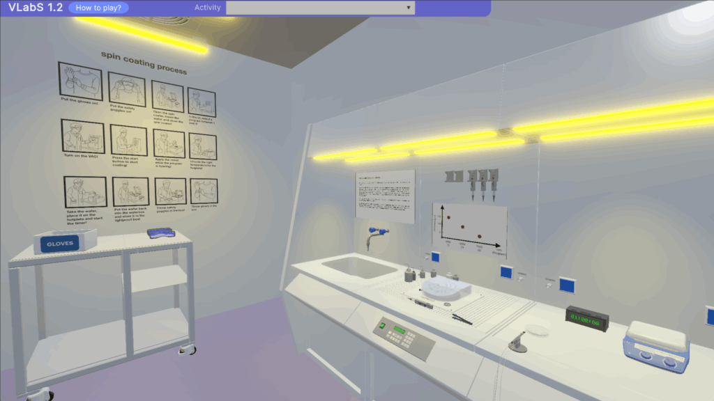
Spin Coating – Applying photoresist to a wafer
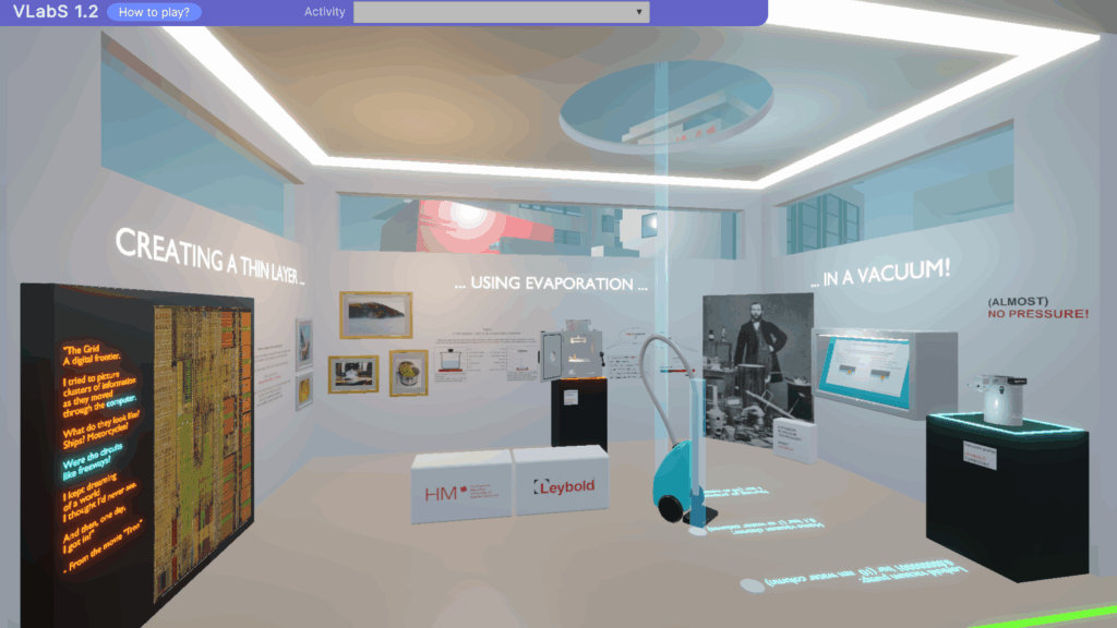
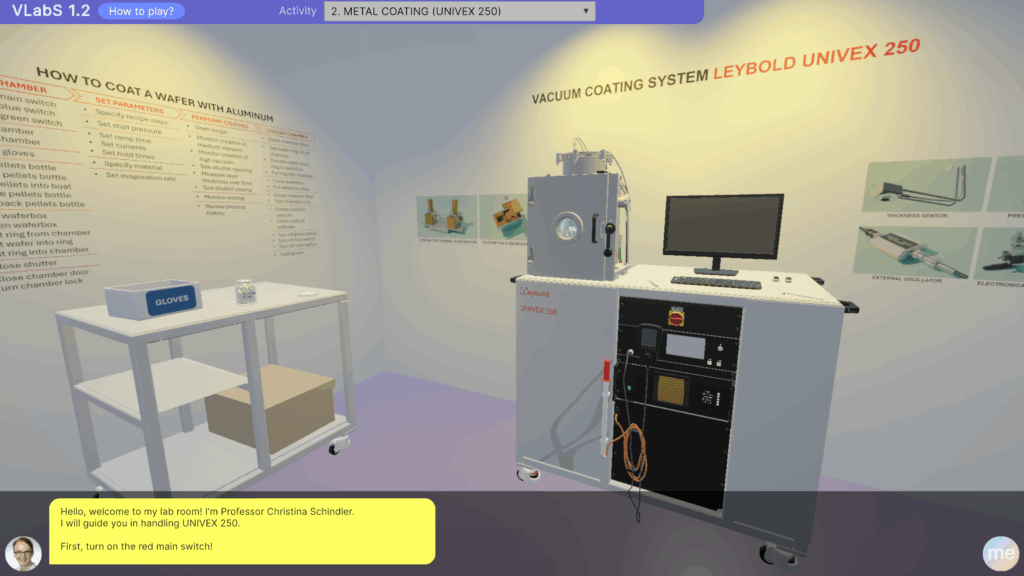
Metal Coating – Understanding metallization in chip production
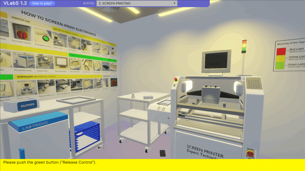
Screen Printing – Depositing patterns using printing techniques
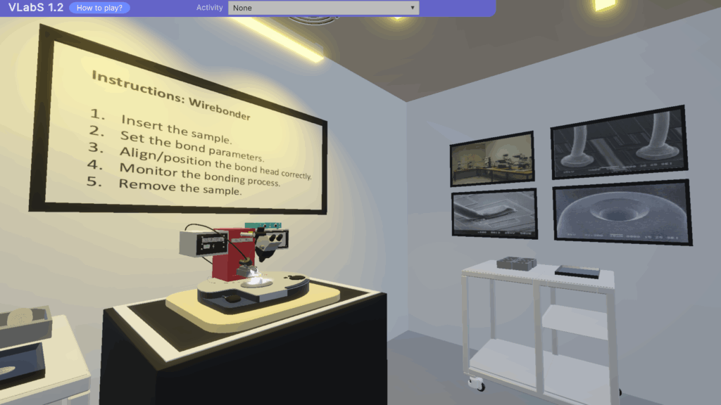
Wire Bonding – Connecting chips to their package using micro-wires
Each module provides authentic animations, equipment layouts, and explanations based on real industrial processes.
Reconstructed Campus Sites
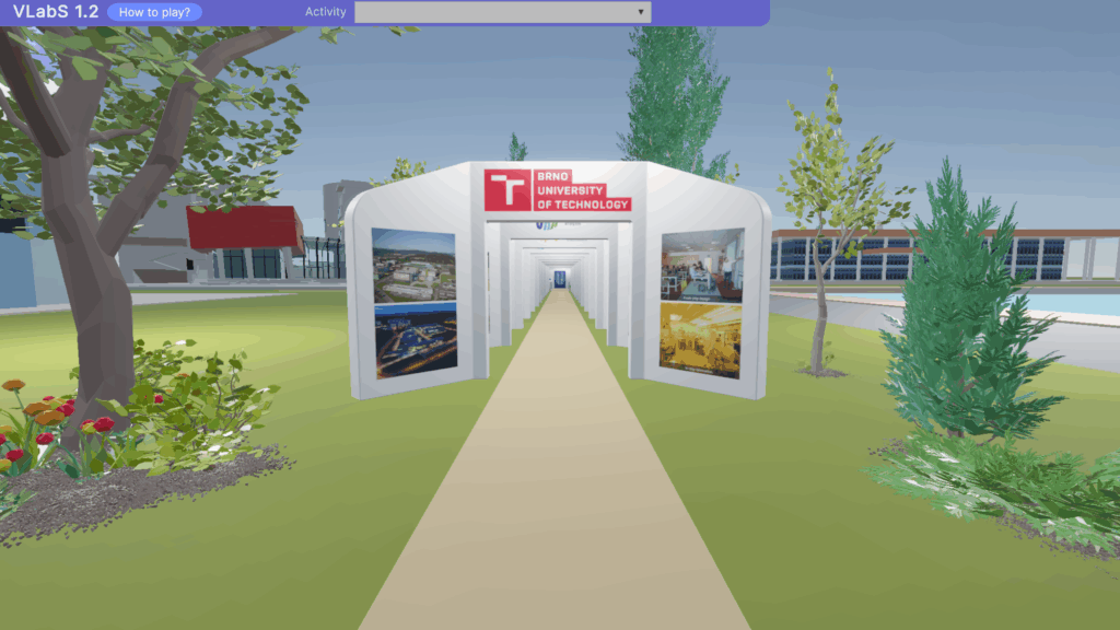
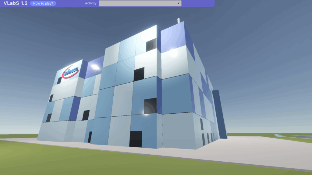
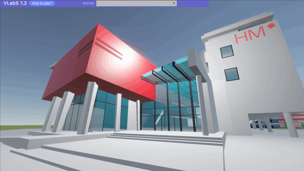
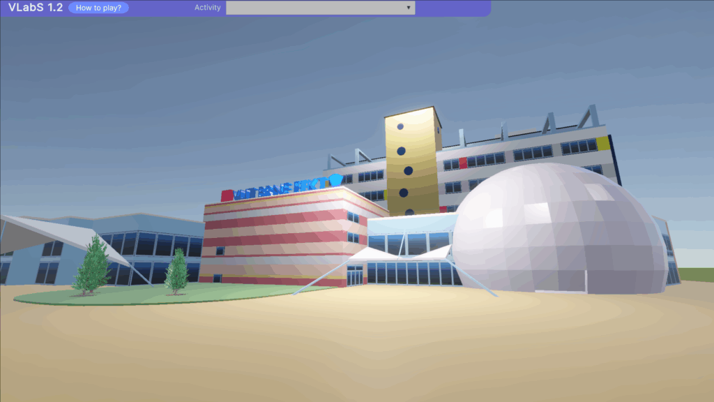
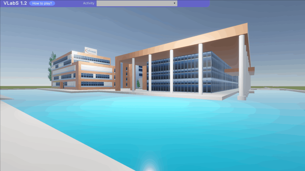
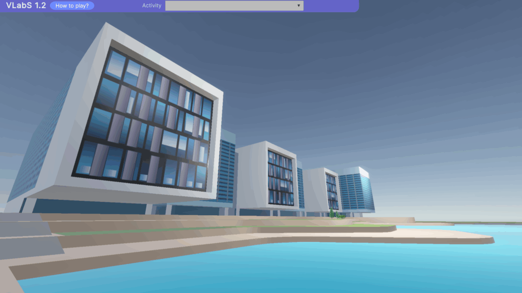
To further connect learning with real-world environments, VLabS includes detailed 3D reconstructions of partner institutions throughout Europe:
- Infineon Villach (Austria)
- University of Applied Sciences Munich (Germany)
- Brno University of Technology (Czech Republic)
- Infineon Neubiberg (Germany)
- University of Southern Denmark (Denmark)
These environments provide orientation, storytelling, and a sense of place—making the lab more engaging and grounded in Europe’s semiconductor ecosystem.
How VLabS Is Built
The virtual lab is being developed using a combination of advanced 3D modeling and real-time game technology:
- Blender is used to reconstruct true-to-life models of semiconductor devices.
- These models are then animated in Unity, enabling interactive experiments and cleanroom simulations.
- The virtual lab building is designed modularly, so new experiments and teaching scenarios can be added continuously.
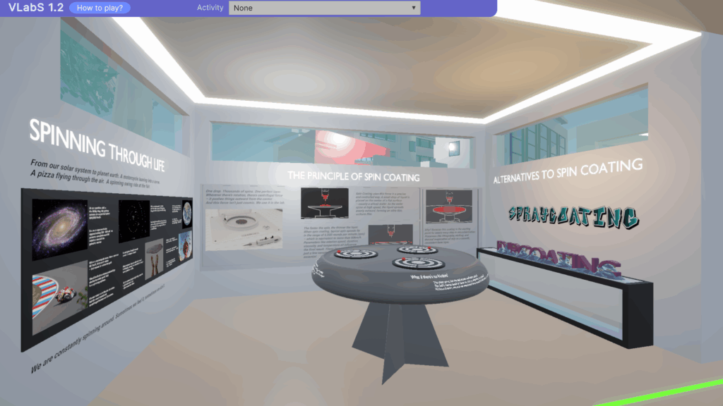
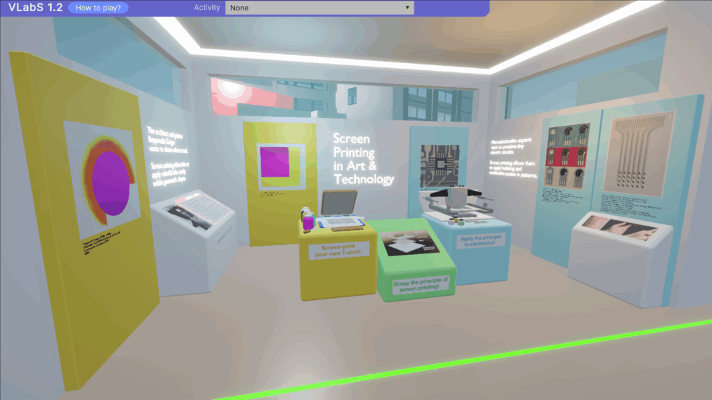
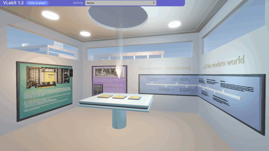
- Gallery rooms located opposite each lab room illustrate connections to everyday life—showing where microchips are used and why innovation in this field matters.
This combination of technical accuracy and creative storytelling is central to making semiconductor topics understandable and exciting for learners with different backgrounds.
Why VLabS Matters
Semiconductors are at the heart of Europe’s digital future—but the technology behind them is often seen as complex and inaccessible. VLabS tackles this challenge by:
- Making chip fabrication tangible and interactive
- Providing low-threshold entry into advanced STEM topics
- Encouraging young learners to explore semiconductor studies and careers
- Supporting teachers and lecturers with a flexible, modular digital tool
By blending education, gamification, and real industrial environments, VLabS helps bridge the gap between the classroom and the cleanroom.