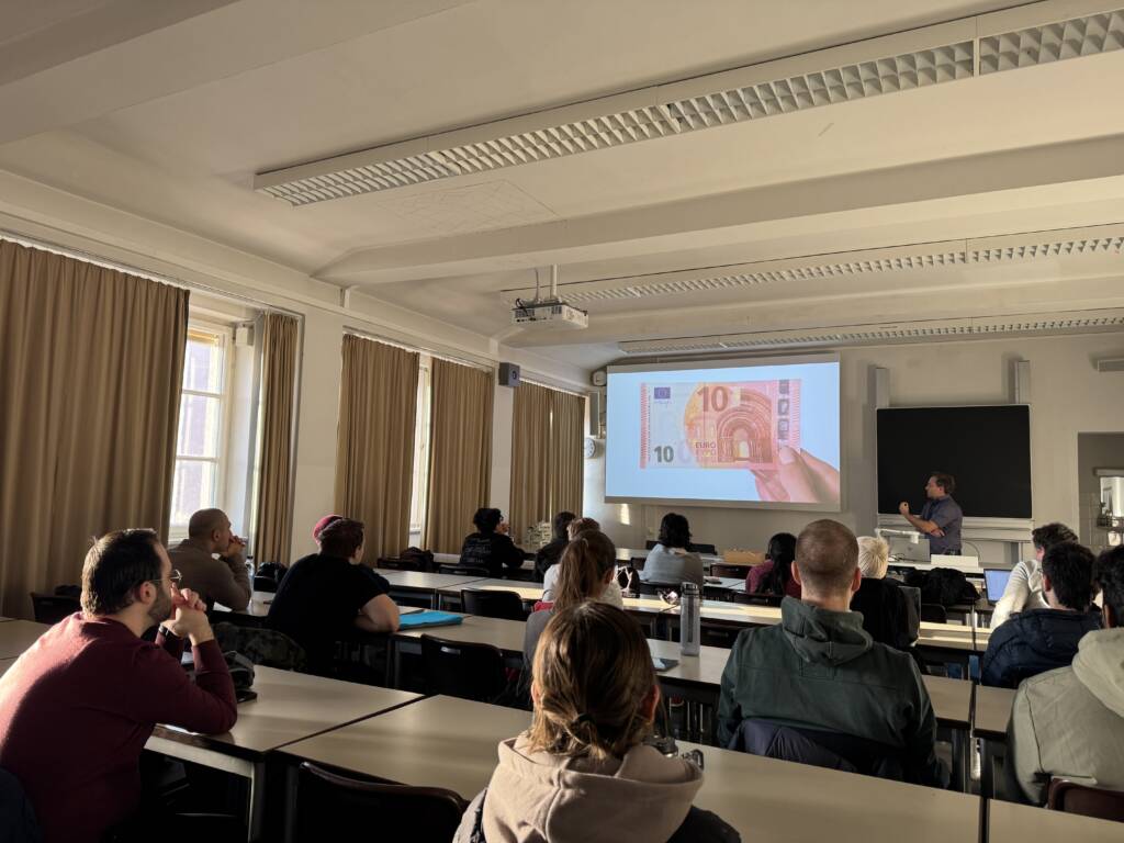
How do micro- and nanostructures end up on something as familiar as a banknote? And what does semiconductor technology have to do with the cash in our wallets?
Students of the Master’s programme Micro- and Nanostructures at the University of Applied Sciences Munich recently had the chance to explore these questions in depth during a guest lecture by Christian Stöckl, development engineer at Papierfabrik Louisenthal.
What Is VLabS?
VLabS is a work-in-progress virtual laboratory that functions like a computer game. Players move through a digital cleanroom environment and experiment with tools and processes used in chip fabrication. Each station is modeled after real semiconductor equipment, allowing learners to understand complex processes through interactive, hands-on exploration.
VLabS is targeted at the general public, high-school students, and university students, giving each group an intuitive entry point into the world of micro- and nanotechnology.
Where Paper Meets Nanotechnology
Papierfabrik Louisenthal is a global leader in banknote and security paper manufacturing. In his talk, Christian Stöckl provided students with an exciting look behind the scenes – showing how high-end security features on banknotes rely heavily on technologies rooted in micro- and nanotechnology.
These include:
- Optically variable micro- and nanostructures
- Lithographic processes inspired by semiconductor manufacturing
- Holograms and dynamic optical effects
- Micro-lens arrays and surface structures that imitate curvature or produce colour-shifting effects
As Stöckl explained, modern banknotes use a combination of touch, sight, and movement to help distinguish real currency from counterfeits. Many of the security features consumers recognize – colour shifts, shimmering elements, holographic effects – are based on extremely fine microstructures manufactured with high precision.
Nature often acts as a teacher: the brilliant colour effects on the wings of blue butterflies, for example, have inspired designs for similar nanostructures on banknotes.
From Student to Innovator in Security Technology
Christian Stöckl is no stranger to the university. He completed his Bachelor’s degree in Physical Engineering and later earned his Master’s degree in Micro- and Nanotechnology here in 2012. Today, he works at Louisenthal’s site at Tegernsee in the department for optical effects, where he develops processes for next-generation banknote security features.
His daily work involves precisely those lithographic techniques commonly used in semiconductor manufacturing – yet applied to paper and polymer films at high volume. The challenge:
🔹 on one hand, creating nanostructures so complex that they are nearly impossible to counterfeit,
🔹 and on the other hand, producing them reliably and cost-effectively using large-scale roll-to-roll processes.
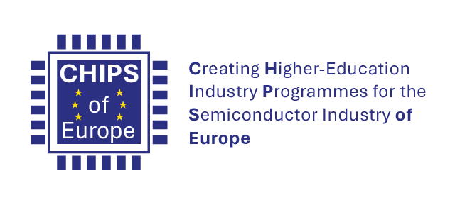
Part of the CHIPS of Europe Project
The lecture was part of CHIPS of Europe, an EU-funded initiative dedicated to strengthening semiconductor education and building closer ties between universities and industry. The talk demonstrated impressively how interdisciplinary semiconductor-related technologies truly are. They go far beyond silicon wafers – extending into fields like security printing, optical design, and materials engineering.
Christian Stöckl’s insights showed the students one thing clearly:
Semiconductor technology is everywhere. Even on a banknote.